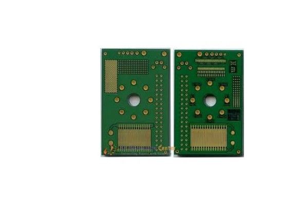
FR-4 Multilayer impedance controlled rigid flex pcb 0.075mm Min. Line
Quick Details
|
Brand Name: |
OEM |
Number of Layers: |
4-Layer |
Base Material: |
FR4/Copper base |
|
Copper Thickness: |
1 OZ |
Board Thickness: |
1.6mm |
Min. Hole Size: |
0.15mm |
|
Min. Line Width: |
0.075mm |
Min. Line Spacing: |
0.075mm |
Surface Finishing: |
HASL |
Specifications
FR-4 material
specialized in pcb
China manufacture
pcb connector Application
Products are applied to a wide range of Hightech industries such as: LED, telecommunication, Induction cooker
pcb board computer application, lighting, game machine, industrial control, power, automobile and high-end
consumer electronics, ect. By unremitting work and effort to the marketing, products exports to American,
Canada, Europe counties, Africa and other Asia-pacific countries.
What can we do for you ?
We can provide the products pcb connector such as 1 to 30 layers,RoHS Compliant, UL-listed,Fine line 0.07mm min,Microvia 0.2mm min,Blind Vias & Buried Vias,Surface as Chemical Tin, Silver, Gold ,HASL,Falsh Gold,HASL lead free,For high current: 3 OZ Copper,Special material: AL Based,Rogers,FR4,FR4 HTG,CEM-1,SMD-stencils,A.O.I. (Automatic Optical Inspection),X-Ray (innerlayer misalignment control),Impedance Control with Testprotocol pcb assembly .
pcb connector Advantage
1.Excellent quality and reasonable price .
2.PCB with high quality. strict test through AOI (Automated Optical Inspection),QA/QC, Flying Proble Test,
E-test fixture
|
Productivity |
|
Item |
Technical standards |
|
Rise |
1-30layer |
|
Material |
CEM-1,CEM-3,FR-4,FR4 TG170,TG180 ,HALOGEN FREE |
|
Lamellar |
0.2mm-3.20m(8mil-126mil) |
|
Minimum thickness |
0.1mm(4mil) |
|
Thick copper |
0.5-6 OZ |
|
Min line w / s |
0.075mm(3mil) |
|
Min Hole Side |
0.20mm(8mil) |
|
Min aperture Chong |
0.9mm(35mil) |
|
Tolerance |
Hole drilling bit |
±0.075mm(3mil) |
|
Linewidth |
±0.05mm(2mil)Or width of ± 20% |
|
Aperture |
PTH±0.075mm(3mil) |
|
NPTH±0.05mm(2mil) |
|
Shape tolerance |
Milling Machine±0.15mm(6mil) |
|
Punch±0.10mm(4mil) |
|
Warp |
0.70%-1.5% |
|
Pad surface treatment |
Nickel/Gold Finger Plating/Flash Gold /Entek/LEAD Free Hal |
|
Insulation Resistance |
10k-20MΩ |
|
Conduction resistance |
<50Ω |
|
Test voltage |
300v |
|
V Engraved |
Panle size |
110*100mm(min.)660*600mm(max.) |
|
Thickness |
0.6mm(24mil)min. |
|
Retention of the thickness |
0.3mm(12mil)min. |
|
Tolerance |
±0.1mm(4mil) |
|
Width |
0.50mm(20mil)max. |
|
Trough to a line |
0.5mm(20mil)min |
|
Trough |
Slot size tlo.≥2WTolerance |
PTHL:±0.15mm(6mil) |
|
W:±0.1mm(4mil) |
|
NPTH: ±0.125mm(5mil) |
|
W: ±0.1mm(4mil) |
|
To circular from the hole |
PTH Hole: 0.13mm(5mil) |
NPTH Hole: 0.18(7mil) |
|
MLB |
Circular deviation |
0.075mm(3mil) |
|
Deviation between layers |
4 layers: 0.15mm(6mil)max |
|
6 layers: 0.025mm(10mil)max. |
|
Aperture to the smallest distance from the inner circle |
0.25mm(10mil) |
|
To circular from the hole |
0.25mm(10mil) |
|
Thickness Tolerance |
6 layers: ±0.15mm(6mil) |
|
6 layers: ±0.15mm(6mil) |
|
Characteristic Impedance |
60Ω±10% |

 Your message must be between 20-3,000 characters!