Introduction
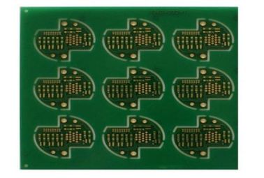
Rigid flex printed circuit boards are boards using a combination of flexible and rigid board technologies in an application. Most rigid flex boards consist of multiple layers of flexible circuit substrates attached to one or more rigid boards externally and/or internally, depending upon the design of the application. The flexible substrates are designed to be in a constant state of flex and are usually formed into the flexed curve during manufacturing or installation.
Rigid flex designs are more challenging than the design of a typical rigid board environment, as these boards are designed in a 3D space, which also offers greater spatial efficiency. By being able to design in three dimensions rigid flex designers can twist, fold and roll the flexible board substrates to achieve their desired shape for the final application's package.
Material Types
FR-4, CEM-1,CEM-3, IMS, High TG,High Frequency, Halogen Free,Aluminum base, metal core base
Surface Treatment
HASL(LF), Flash gold, ENIG,OSP(Lead free compatible), Carbon ink,
Peelable S/M, Immersion Ag/Tin, Gold finger plating, ENIG+ Gold finger
Production Process
Whether producing a rigid flex prototype or production quantities requiring large scale rigid flex PCB fabrication and PCB assembly, the technology is well proven and reliable. The flex PCB portion is particularly good in overcoming space and weight issues with spatial degrees of freedom.
Careful consideration of flex-rigid solutions and a proper assessment of the available options at the early stages in the rigid flex PCB design phase will return significant benefits. It is critical the rigid flex PCB fabricator is involved early in the design process to ensure the design and fab portions are both in coordination and to account for final product variations.
The rigid flex manufacturing phase is also more complex and time consuming than rigid board fabrication. All the flexible components of the rigid flex assembly have completely different handling, etching and soldering processes than rigid FR4 boards.
Application
LED, telecommunication, computer application, lighting, game machine, industrial control, power, automobile and high-end consumer electronics, ect.a

 Your message must be between 20-3,000 characters!
 Please check your E-mail!
  Your message must be between 20-3,000 characters!
 Please check your E-mail!


