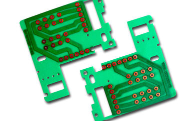
Quick Turn Single Layer PCB Design , Prototype PCB Manufacturer FR4 1 layer 1.6mm thickness
Product Description
> Brand Name: East PCB
> Material: FR4
> Layer Count: 1layers
> Board Thickness: 1.6mm
> Copper Thickness: 1OZ
> Surface Finish: HASL (lead free)
> Solder Mask: blue
> Silkscreen: White screen (top&bot)
> Min drill/pad: 0.1mm/ 0.2mm
> Place of Origin: China
> Certification: UL, RoHS, ISO9001,
ISO14001, TS16949
Requirements and services including:
•Design, technical and advisory services
•Single and double sided (both NPTH and PTH)
•Multlayers
•Hot Tin/Lead Solder
•Lead Free- RoHS
•Gold or Silver Immersion
•Gold fingers
•Electroplated Copper, Tin or Silver
•SMT Stencils
•Peelable mask
•PCB panel laminate supply
•Light Sensitive film laminate
•Electrical testing
•V Scoring
•Budget Prototype Service
•International outsourcing
•UL Certication
•QA Conformance Certification
•Specialist plating thickness measurement certification
Main application:
> Security industry:
intelligent building system, video intercom, DVR, network camera, etc.
> Communication device:
CDMA device, switchboard, access network and broadband transmission facility, etc.
> Electrical equipment:
power monitoring equipment, power dispatching equipment, high-frequency switching power supply, etc.
> Network equipment:
Network server, router, VDSL, etc
> Computer equipment:
Industrial control computer, computer motherboard, etc
> Medical instrument:
Nuclear magnetic resonance instrument (MRI), CT, color Doppler, monitors, etc.
> Cutting-edge technology:
aerospace, missile, radar and other military products
> Consumer electronics:
Digital camera, MP3, car electronic
PCB Capability
| NO |
ITEM |
Technical capabilities |
| 1 |
Layers |
1-28 layers |
| 2 |
Materials |
FR4, Hi-TG, Rogers, FPC, Aluminum |
| 3 |
Board Thickness |
0.2-5.0mm |
| 4 |
Finished Copper Thickness |
1/2 OZ, 1-5 OZ |
| 5 |
Min. line Width/Space |
0.1mm(4mil) |
| 6 |
Min. S/M Pitch |
0.1mm(4mil) |
| 7 |
Min. hole size |
0.2mm(8mil) |
| 8 |
Solder mask color |
green, blue, black, white, yellow, purple, etc |
| 9 |
Silkscreen Color |
white, black, yellow |
| 10 |
Surface Finished |
HAL(lead free), Immersion gold, OSP |
| 11 |
Other Technology |
Gold finger, peelable mask, Non-across blind/buried vias, characteristic impedance control, etc. |
| 12 |
Reliability Test |
flying probe test/fixture test, impedance test, solderability test, hole resistance test, etc. |

 Your message must be between 20-3,000 characters!
 Please check your E-mail!
  Your message must be between 20-3,000 characters!
 Please check your E-mail!


